Overview and Motivation
Sometimes people ask me for a FPGA implementation of MyCPU. My philosophy was and still is that MyCPU shall be
a computer built from discrete logic. But anyway it would be nice to have a kind of MyCPU with a smaller form factor.
So I started thinking about a FPGA version. My aim was to put as much as possible from the MyCPU logic onto a single
board. The board should have the same size like all other MyCPU boards (that is 160x100mm) and it should be equipped with
the MyCPU's backplane connector that enables the use of existing extension boards together with the new MyCPU.
Because of the small size of the new MyCPU I named the project "MyCPU Compact".
MyCPU Compact provides the following functionality:
- MyCPU processor core
- 1MB SRAM and 512kB Flash-ROM
- Two serial interfaces
- PS2 keyboard port
- LCD interface port
- Parallel printer port
- Two IDE interfaces
- Realtime Clock
- Extension port for piggybacks
- 8 digital user inputs
- 8 digital user outputs
- 8 Status LEDs
- Backplane connector
- Full software compatibility to MyCPU v2.3
It is planned to develop a piggyback board that provides the still missing VGA- and Ethernet interface.
The Board
The board is a multilayer-board with 4 layers. Components are placed on both sides. The inner layers are mainly used
for the power supply (1 GND-plane and 1 supply-plane).
Top side:

Bottom side:
Used Technology
The main part of the logic is placed in a Spartan-3 FPGA with 400k gates from Xilinx. A small CPLD (also from Xilinx)
is used to implement the IDE controller and the parallel printer port. Because modern FPGAs require a lower supply
voltage the board uses 4 different voltages: 5V (for the interfaces), 3.3V (FPGA and memory chips), 2.5V (FPGA) and
1.2V (FPGA). Because of the different voltages level-shifters are required to translate between 5V and 3.3V-signals.
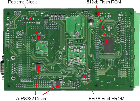
These silicon components are used:
- FPGA: Xilinx Spartan-3 XC3S400-4C in TQFP-144 package
- CPLD: Xilinx XC9572-15 in TQFP-100 package
- Boot-PROM for FPGA: Xilinx Platform-Flash XCF02S
- Flash Memory: Spansion S29AL004D70TFI02 in TSOP-48 package
- SRAMs: Samsung K6R4008V1D (SOJ-32 package)
- RS232 transceivers: MAX3245ECAI
- Realtime Clock: DS1307Z (SO-8 package)
- Level Shifter: 74LVC4245A (dual supply)
- I/O-extension: 74HC595, 74HC166
- Voltage regulators: LT1117, LM2853MH-3.3, LM79L05ACM
The Xilinx parts and the memory chips are hard to obtain. Some components are pretty old and manufacturing maybe stopped
in the near future. But I need these parts because of their packages that can still be soldered by hand.
The board is a multilayer board with four layers. The smallest structure is 6mil, the smallest drill is 0.3mm.
The components are placed on the top and the bottom layer. Signal wirings are mainly done also on the top and the bottom
layer, but some wirings that could not be routed must be put into the middle layers. The two middle layers are used
for GND and power supply. I am using Cadsoft's
Eagle PCB layout tool (vesion 4.16r2)
for my PCB designs.
The FPGA and the CPLD are programmed in the hardware description language
"VHDL". For Synthesis and Place&Route I use
Xilinx ISE WebPACK 11.1. For VHDL source simulation
I use ModelSim PE
and the open-source simulator GHDL.
VHDL Simulation
I am using Mentor's ModelSim for wave form analyses. Because I have only the limited PE version, it is only
possible to do short time simulations up to 100us CPU run time with ModelSim. For longer time simulations I use the
free GHDL simulator. Since GHDL is only available for Linux I have installed Linux in a Virtual Machine on my Windows
Desktop PC. To view the wave form file that is produced by GHDL I use the GTKWave Analyser.
I have simulated the MyCPU boot-up process with GHDL. The testbench writes all data that MyCPU sends over COM1 to the
text file "output.txt". Because it is not possible to send key-strokes to the simulated MyCPU I use a test
script file that is executed by the MyCPU OS kernel after boot-up. The sript executes the commands "ver" and
"mem" and then starts a small basic program that does some floating point calculations.
If you like you can try it out yourself. Download the MyCPU Compact project archive and run GHDL.
Make sure the setings in the testbench are correct. In mycpu_tb.vhd you will find a definition for
"CFGSWITCHES". Make sure the IDE controller and the PS2 keyboard interface are switched off.
Otherwise the boot-up process would take too long. Start the GHDL-simulation by entering "make clean"
followed by "make run NOWAVE=1 TIME=3000ms" in the \vhdl\simulation\ghdl directory.
GHDL will then produce the file "ouput.txt" that should finally look like this:
 [0;37;40m[H[2J
 FOUND: Memory Extension Board
 FOUND: Interrupt Controller
 FOUND: RS232 Interface (UART)
 FOUND: Parallel Printer Port

 Romdrive installed (drive 15)
 starting 15:/init
 MyCPU boot script started
 Kernel  version 2.18
 k-Shell version 2.1
 MicroFS version 2.4
 Basic   version 3.0

 free program ram     : 30803 bytes
 free paged data ram  : 966656 bytes
 free user zeropage   : 32 bytes
 free zero/stack pages: 89
 [0;37;44m[1;36;44m[H[2Jsin( .1[C) =  .0998334167[C
 tan( .1[C) =  .100334672[C
 log( .1[C) = -2.30258509[C
 sin( 1.5[C) =  .997494987[C
 tan( 1.5[C) =  14.10142[C
 log( 1.5[C) =  .405465108[C
 sin( 1.9[C) =  .946300088[C
 tan( 1.9[C) = -2.92709752[C
 log( 1.9[C) =  .641853887[C
 ti = 21[C
 ti = 22[C
 ti = 22[C
 ti = 22[C
... et cetera ...
|
Please ignore the "[C" garbage characters. They are the remainder of the
escape sequence that moves the cursor right.
Special Tools
FPGA and CPLD programming:
I use the Xilinx
"Parallel
Cable III model DLC5" (PDF) for programming the logic chips. If you cannot obtain
this cable it is not difficult to build your own one. The pdf file shows also the (simple) schematics
of the cable. But note that you must have a working LPT parallel printer port to use this cable!
Flash Memory programming:
The Flash Memory is programmed in-circuit. This requires that the FPGA is programmed and is working correctly.
I have implemented a simple "RS232 to memory-interface converter" in the FPGA. To activate this converter
(also called "Debug-Mode") the DIP-switch 7 on the board must be switched on. The Flash-Memory can then
be accessed through the COM1-port. The MyCPU Compact board is connected via a RS232 Null-Modem cable to a PC and
a special program on the PC does the rest.
This is the command line I use to program the OS-image files IC14.bin and
IC15.bin into the Flash Memory chip:
flashprog com1 -f IC14.bin IC15.bin
The flashprog-tool is contained in the MyCPU Compact source file package that can be found in the
download section.
The ROM image files IC14.bin and IC15.bin are contained in the "Memory Unit Selfbuild Guide", see the
guides section.
Tools for SMD soldering:
A fine solder iron, soft solder flux, many solder wick, some forceps, valium and good eyes ;-)
Board Configuration
MyCPU Compact provides 8 DIP switches for configuration purpose. The meaning of the switches is shown in the table below:
|
Switch
|
Function
|
|
1
|
enable internal Interrupt Controller
|
|
2
|
enable internal Multi-I/O-Unit
|
|
3
|
enable PS/2-Interface in Multi-I/O-Unit
|
|
4
|
enable internal IDE Controller
|
|
5
|
reserved
|
|
6
|
LCD configuration switch 1
|
|
7
|
LCD configuration switch 2
|
|
8
|
enable program and debug modus
|
|
Some hints about configuration:
- The default configuration is switches 1,2,3,4 "on" and switches 5,6,7,8 "off".
- It is possible to use MyCPU Compact together with other peripheral boards. For example, if you are using
MyCPU Compact with an external IDE Controller board, you must set switch 4 to "off"-position.
- If you want to load an Operating System image into the on-board Flash-ROM memory by using the "flashprog" tool,
you must set switch 8 to "on"-position.
Attention: Be aware of the position of the DIP-switch when soldering it. Switch 1 is near to the
switching regulator / power supply and is connected to the signal "DISP-DATA0".
The switch is swapped on my prototype, thus the pictures on this webside are no reference!
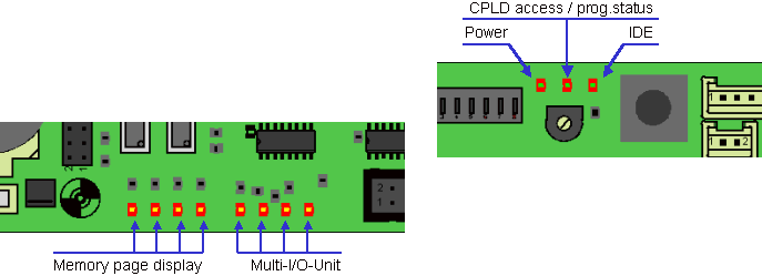
Meaning of the LEDs
The board is equipped with several LEDs:
Status Report
2010-08-24
VHDL sources updated - now working with Xilinx ISE 12.2. There was a problem with a timing constrain (the internal
data bus was constrained as a multicycle path), so I was forced to re-structure the code. The result is, that only a
simple "period" timing constrain is needed. Furthermore the FPGA can be clocked higher, now with up to 34 MHz.
And the last improvement is the faster internal memory access. A load/store from/to internal memory (stack, zeropage)
lasts 3 FPGA clock cycles in the old design, now the memory is accessed in only two cycles.
The download link for the updated VHDL source can be found at the bottom of this page.
2010-04-06
I have found a bug in the LCD Interface. I did a bad mistake when resetting the logic that controls the LCD write timing.
The result of this error was that it was no more possible to write to the registers inside the LCD.
This error appeared and disappeared at different room temperatures. Very ugly! But fixed now :-)
2010-03-16
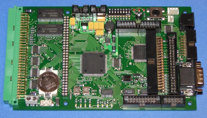
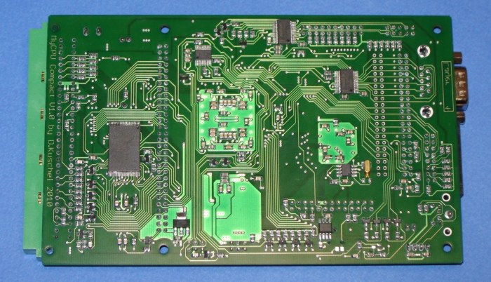
All errors fixed. All tested, all interfaces work fine. Here are the latest pictures of MyCPU Compact:
Top side:
Bottom side:
2010-03-12
I am finished with soldering. First tests were successful, the PCB has no errors.
My baby is alive! MyCPU can boot, but there are still some errors in the VHDL code.
The interrupt-controller and the PS2-interface do not work properly.
Some new pictures of the board will follow soon.
2010-03-07
I have soldered some more parts. Work is still ongoing.
2010-03-02
Got the board. The most difficult parts (FPGA and CPLD) were just soldered by me.
2010-02-08
The board was ordered. Board manufacturing takes around three weeks.
January 2010
I have finished the schematics.
I ordered all silicon parts because I had to check their footprints.
Then I started with routing the board.
December 2009
The VHDL code is programmed and simulated. The MyCPU core is working and boots the Operating System.
I draw a first draft of the schematics.
File Download
MyCPU Compact Files:
Tools:
|