|
|
|
"MyCPU" is a homebrew CPU that was primary
developed for fun. It is a simple 8-bit processor that is completely built
with simple discrete logic gates of the 74xx CMOS series. Over the years
the project has grown, and now MyCPU is the brain of a real Personal
Computer. The project is totally open source, and everybody is invited to
participate and contribute to the project.
Currently the computer consists of the
following main parts:
8-bit processor, consisting
of around 65 integrated circuits placed on 5 euro cards
Interrupt Controller Board, providing 7
edge-triggered, maskable interrupts and 1 timer interrupt
Memory Unit with up to 1 MByte bank
switched RAM and 160 kByte ROM
Multi-I/O-Unit with keyboard, LCD, 2 x RS232 and
one parallel printer port interface
IDE Controller Board with RTC/CMOS and
two IDE ports for up to four IDE devices / harddisks
VGA Graphic Unit providing 16 colours
and 80x50 character text mode and several graphic modes
Ethernet Controller with 10BaseT interface
to allow simple connectivity to the Internet.
|
|
The processor performance is around 1 MIPS (where an integer has 8 bit). The
CPU can be clocked up to 8 MHz. The speed is limited by the slow EPROM's
used in the CPU design and by the slow external components. Because of the
cable length and mismatched line impedance the processor bus cannot be
clocked higher than 4 MHz, making it to the bottleneck.
The fully equipped
system has a power consumption of less than 3.5 Watt. This is due to the
fact that only CMOS chips are used and the power dissipation at 8 MHz
clock frequency is near zero. Most power is consumed by the VGA Unit (1.3
Watt) that runs at 25 MHz.
The MyCPU is not only a hardware but also a
software project. Today much software is available. The Operating System
that resides in an EPROM is completely written in assembly. The OS is a
mixture of DOS, Unix and Commodore 64, and provides most of the well-known
commands to manage hard disks. MyCPU has its own file system that is able
to handle up to 8 disks or partitions. Drivers for additional external
hardware components like the Ethernet Controller can be loaded from disk.
Furthermore MyCPU OS comes with a build-in basic interpreter that is
compatible to the
|
| |
basic interpreter of Commodore 64. Old pure basic programs that were written
for C64 can be run on MyCPU without modification.
MyCPU can be programmed in three more programming languages: For the fans of
higher-level languages a "C"-Cross-Compiler is available. And hardcore freaks can write
their programs directly in assembler or in the esoteric programming language
"brainfuck" (MyCPU OS comes with a build-in JIT compiler for brainfuck).
The following application software is currently available for MyCPU: Basic
interpreter, brainfuck compiler, assembler, text editor, games and demo's, networking
software like HTTP web server and a Telnet demon. And of course there are some more
tools available that make life with MyCPU more convenient.
Technical data of MyCPU
- 8-bit processor, Harvard architecture
- 16 bit address bus, 2x 64 kB address range
- runs up to 8 MHz
- 8-bit integer performance is around 1 MIPS
- 247 OP-Codes, 9 reserved for future use
- 14 addressing modes
- 256 byte stack memory
- 1 non-maskable software interrupt
- 1 maskable hardware interrupt
- 65 integrated circuits on 5 boards
|
|
|
|
|
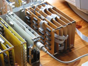
Where "MyCPU" stands for the processor itself, I use the term "MyCPU System" for
the whole home-brew computer. The fully equipped MyCPU System currently consists
of the following components (compare with figure[1], from left to right): MyCPU
(5 boards), Interrupt Controller (1 board), Memory (2 boards), I/O (3 boards), IDE
Interface (1 board), VGA Graphic (6 boards), Ethernet Controller (1 board) and the Power
Supply (1 board). The system provides this interfaces to the outside world: PS/2 Keyboard,
alpha-numeric LC-Display, 2 RS232 Interfaces, Parallel Printer Port (Centronics),
8 universal inputs and 8 universal outputs, VGA graphic interface (RGB, 15 pin high
density Sub-D) and 10 MBit Ethernet (RJ45 twisted pair). Because I have not written the
FTP server software yet, data communication with a PC is still done through a serial link
via RS232 and special software. But note: You can now trash your PC since there is
|
|
everything available that you need to work stand-alone with the MyCPU System ;-).
For example there is an assembler program available that runs on MyCPU and
produces code for MyCPU. The evolutionary step is that the
|
|
assembler can assemble itself on MyCPU. So you can write software for MyCPU on MyCPU, and
you are no more required to use a PC for special tasks.
|
Figure 1: Fully equipped MyCPU System
|
|
A closer look to the processor
|
|
|
|
|
The MyCPU processor (depicted in figure[2])
is a complex microcode machine (CISC), like
any modern processor today. The internals of my CPU are shown in
figure[3]. The core
of the processor is the microcode engine that controls the data flow from and to
the registers and arithmetic components. The processor has only 5 universal and 1
special purpose register:
A, X, Y, P and SP are universal 8-bit registers,
whereas the Program Counter (PC)
|
|
is a special purpose 16-bit register whose contents can be incremented
by one through a dedicated signal.
The P-register is only an internal register
used by the microcode to store temporary data and is not visible to assembly
programs.
In my implementation the microcode covers many commands
and addressing modes of the good old 6502 processor, but MyCPU is
|
|
not binary compatible to it. The microcode can be adopted to simulate
other processors like Z80, 8051 or whatever; the only limitation is the
number of internal CPU registers. For Z80 or 8051 it becomes necessary to
store registers in external memory. The microcode was developed with the
help of a "macro language".
The Microcode-Compiler is written in "C" and does
also some validity checks and optimisations on the generated microcode. For example
the OP-Code "CLA" (clear accumulator) is constructed from the following micro-OP's:
fetch_opcode_and_increment_pc, move_const0_to_accu, update_flags, next_op.
The processor design is optimised for speed. With easy to obtain parts like usual EPROM's
with 100ns propagation delay and the usual 74HCxxx series of logic gates MyCPU can
be run with at least 4 MHz. It is possible to clock MyCPU even higher, but than some
parts must be replaced, e.g. faster EPROM's are needed and some 74HC-chips must be
replaced by faster 74AC-chips. I have successfully run a MyCPU at above 8 MHz, but
that is only possible with a short bus length and a reduced number of peripheral boards.
My goal was to have a fast and efficient processor that requires as less parts as possible by
providing a superior high processing power. The MyCPU design is a good compromise.
Of course it would be nice to have a 16-bit processor with 32-bit address
range, but this would double the amount of required parts.
|
Figure 2: MyCPU processor cube
|
|
|
|
The MyCPU System is equipped with 1 MB RAM and 160 kB ROM. Since MyCPU has
only an address range of 16 bit (that means 64 kB of linear memory can be accessed), it
is necessary to do some bank switching to allow MyCPU to access all the memory. The ROM
|
|
is partitioned into chunks of 32 kB. The EPROM that contains the Operating System
Kernel is always visible and is mapped to the address range 0000h - 7FFFh. The other
four 32 kB ROM partitions can be mapped to 8000h - FFFFh. These ROM partitions
|
|
contain the filesystem driver, the shell and the Basic Interpreter. The RAM can also be mapped
into the area between 8000h and FFFFh. Thus, a program that is loaded from disk can
have a maximum size of 32 kB. That is why it is not possible to run Linux on MyCPU
(there are some other limitations also, e.g. Linux requires at least a 16 bit processor).
There are some more special features on the memory board: The RAM can be split into
16kB chunks that can be paged into the area 4000h to 7FFFh. Furthermore the two lowest
256 byte pages, which are the zero-page and the stack-page, can also be bank-switched.
This allows the use of more stack memory and enables MyCPU to run multitasking
operating systems. I have successfully ported the RTOS " Pico]OS" to MyCPU.
OK, that is only half of the truth. Remember MyCPU has a Harvard like architecture,
except that there are no two separate buses to access program and data memory. It's
more like the 8051; MyCPU supports two different read signals, one for code- and one
for data-memory. If you are interested in how memory bank switching really works
please read the Memory-Selfbuild-Guide that can be found on my website.
Physically the Memory Unit consists of two boards: The baseboard provides
512 kB RAM and 160 kB ROM. The optional extension board adds 512 kB
more RAM and a second paging unit.
Figure 3: Internal architecture of MyCPU
|
|
|
A minimalist Computer System
|
|
|
|
|
Figure[4] shows how a minimalist computer
system with MyCPU looks like. At the left side you see the MyCPU cube. The two
other boards are the memory baseboard with 512 kB RAM and the RS232 interface
board that mainly consists of two commercial 16C550 UART's and some glue-logic. User
communication is done with a terminal program like Hyperterm on MS Windows
or minicom on Linux. A second serial link is used for file transfer between MyCPU
and a PC. The PC must run special server software for this purpose. When the System
is powered on it searches for boot files on the PC. The user can choose one
of four
|
|
software packages that is then loaded into a RAM-disk on MyCPU.
With this minimalist computer system the user can write and save texts, write
Basic programs, write and assemble Assembler programs, play games and
run network services like the http server and Telnet over a SLIP link.
Figure 4: Smallest possible MyCPU computer system
|
|
|
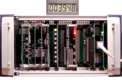
Figure 5: MyCPU Webserver for www.mycpu.eu
|
| Want to build your own MyCPU Computer?
|
|
Since the MyCPU Computer is completely open source you
can get all the schematics and software from my website.
You should start with building the MyCPU
itself and the memory board. For this purpose you need
to download the "MyCPU Selfbuild Guide" and the
|
|
"Memory Selfbuild Guide".
When the set-up of CPU and memory works as expected, you can continue to
build the serial interface board. The fourth board would be the Interrupt Controller
which is required to be able to use the next boards that are: Keyboard/LCD,
IDE Controller, VGA and Ethernet (in any order). Are you interested? If yes, you
may also try out the MyCPU Emulator that can be downloaded from my website
(go to "all downloads" and scroll down).
|
|
|
About the history of MyCPU
|
|
|
|
All had begun in February 2001.
I was learning for my diploma examination in digital
electronics and got bored. I wanted to do something productive with the knowledge
I just obtained. So I decided to construct an electronic calculator machine by using only
fundamental digital gates of the 74-TTL series from which I still had some hands
full in a drawer. At this point it was still nothing special to construct a calculator,
many people would have done this before. It was just an education project for me.
Figure [6]: MyCPU in an early phase. You see the prototype of the
VGA Graphic Unit and besides the Multi-I/O-Unit and the Interrupt Controller.
Which way to go?
Because I already had some experience with the very simple but powerful
6502 CPU, the idea was not to implement the calculator algorithms in hardware but
to construct some programmable machine that should be similar to the 6502. If I could
port the Commodore 64 Basic Interpreter to my machine I would get the floatingpoint
routines for my calculator for free.
This article was printed in
Embedded Projects Journal 03.
|
|
8 bit are enough!
To keep the design as simple as possible 8 bit should be enough for
my machine. Maybe you still remember the Commodore 64 and the powerful games and
demos that ran on it. And this with only 64 kB RAM and less than 1 MHz clock frequency.
That should be possible for my machine, too. My philosophy was and is until today to
use only the simple gate parts. No higher integrated components like GAL's, PAL's
and FPGA's are allowed in my design (this would be too easy and was already
done by many other people). The only higher integrated parts that are permitted
are EPROM's because I needed them to store the calculator program anyway.
How to start?
I sketched the schematics on a piece of paper. The draft of the CPU was
finished within two weeks (while I was still learning for my examination). My idea was
to have a micro code based machine. The advantage is that only a few components
are required. The core logic would reside in a re-programmable EPROM. And because
EPROM's are so universal I also constructed the ALU (Arithmetic Logic Unit) with some
big EPROM's that are simply used as lookup-tables. Thus an 8x8-bit multiplication
can be done within only one clock cycle.
Simulation!
But before I would start constructing the processor in hardware
(what would be an exhausting task) I wanted to test my design. My approach was to
write a CPU emulation in the programming language "C". Version 1 of the emulator
simulated every single gate of the processor, including the timing constraints. The
result was that the design was functional!
|
|
What's with software?
The first emulator simulated the processor (gate by gate), 32
kB ROM and 32 kB RAM. User interaction was done by a simulated serial terminal.
The test software simply read some input from the terminal and outputted
it immediately again. The first "stupid" version of my today's kShell was born!
(This was around April 2001; I already finished my diploma with best degree).
And now: Hardware! Because all went so fine I started constructing "my CPU"
in hardware. The first set-up consisted of the CPU, a memory board and a couple of
LED's for I/O. As next I constructed the interrupt controller and the RS232 I/O board.
The keyboard interface and the VGA Unit followed, and at the beginning of 2002
I had a fully featured "Personal Computer" on my desk.
A friend of mine was so enthused of my project that he recommended
me to share the project with others. So I started my website yet in September 2001.
In the following years
I improved the design and wrote the self-build guides. I spent
much time with developing the application software. Even today I am not finished with
the CPU design, and I will possibly never be. There are still too much things to improve.
My slogan is: "Others have a model railway in their cellar, I have my CPU instead."
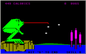
Figure [7]: MyCPU running an old Basic game by Commodore.
|
My name is Dennis Kuschel, I am 32 years old, I live in Bremen / Germany and have studied electronics
on the technical college in Bremen. Currently I am working as hardware engineer for space products at
Astrium in Bremen. Website: http://www.mycpu.eu , Email: dennis_k@freenet.de
|
 |
|